The new Semiconductor Packaging education program, that was developed by Hogeschool Arnhem en Nijmegen (HAN) and Chip Integration Technology Center (CITC) has started today. The education program closes the gap between study and work. The launch of the course is a big step forward for CITC.
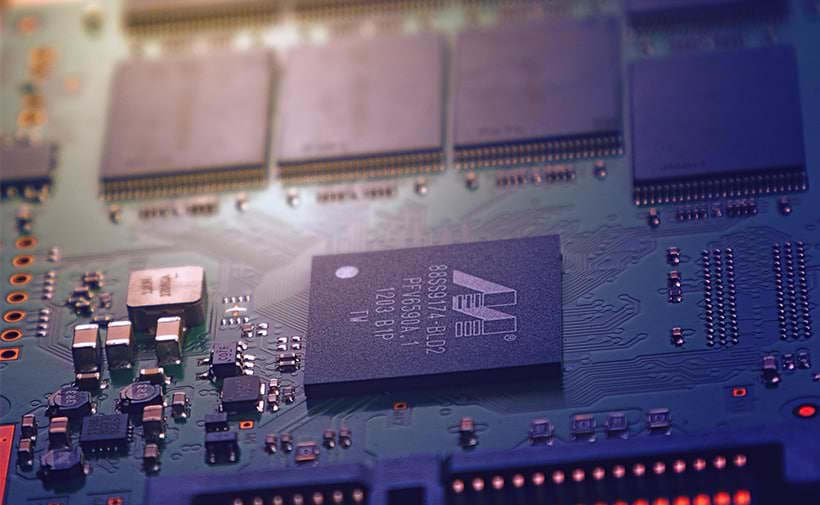
Heterogeneous integration and advanced packaging – stacking and packaging of chips – is essential for connecting chips and protecting them. Chip Integration Technology Center (CITC) develops new technology to make the chip shell smaller, better and cheaper. The innovation center thus plays an important role in smartphones, cars and operating room of the future, for example.
Access to innovation, infrastructure and education
CITC bridges the gap between science and industry, bringing together knowledge in the field of materials, machines and semiconductors. Nijmegen is the home city for large chip companies, such as NXP, Ampleon and Nexperia. In the surrounding area there is an extensive network of companies active in the semiconductor industry. CITC brings these worlds together: entrepreneurs, scientists and young talent join forces and work on new packaging and integration technologies for chips. CITC not only offers access to innovation and infrastructure, education is also one of the important focus areas.
Alderman Monique Esselbrugge from the municipality of Nijmegen is very pleased with the development of talent at CITC. “I talk to many entrepreneurs who are desperate for well-trained, but certainly also immediately deployable employees. CITC can build that bridge to the market by involving students in the research projects and providing training. The fact that the institute guarantees new employment, collaboration with SMEs and supporting start-ups is an important reason for me to fully support this project.”
New Semiconductor Packaging education program
The new Semiconductor Packaging training is tailored to the specific needs of the companies involved and focuses on both students and employees of companies. The 5-month part-time training covers all aspects relevant to the field of semiconductor packaging, both theoretical and practical. The training includes a practical assignment that will be carried out on the premises of a semiconductor company or at CITC. The module was created in collaboration with HAN, CITC and its partners NXP, Nexperia, Ampleon, TU Delft and TNO.
Joep Stokkermans, Director of Innovation Equipment & Automation Technologies of Nexperia emphasizes the importance of the training for the Chip companies: “Nijmegen is home to global players in the Chip industry where innovations in technology and materials follow each other very quickly. Whether it concerns photonics, 5G, autonomous driving, electric cars or IoT, wires must be connected to the chip and a robust package is needed around it. Chip Packaging technologies are often already quite specific, you need a certain domain knowledge for that. The HAN-CITC Packaging Minor offers this domain knowledge in a thorough training; exactly what we as Chip companies need. It offers thereby concrete career prospects to young talent and company employees; a solid theoretical basis supplemented with practical assignments from the industry. A great opportunity to participate in the high-tech kitchens of our Chip companies during your training.”

